Grabbing LCD display: PCB design, layout, routing
This is the third part of my LCD display grabbing adventure, the first part is here, and the second part is here.
We got the basic LCD grabber working, and we selected chips and a general design for the system. It’s now time to design a PCB. I tried a flow where Claude works on a design doc for the PCB, creates a SKiDL script to describe the circuit, generates a netlist, and then this human does the PCB layout. This is quite different from a usual EE flow where one would start with schematics.
AI-first PCB design
In a previous post, I went for a more “classical” PCB design flow, starting with schematics (which I failed to generate with Claude), then moving on to PCB layout.
Here, I tried a flow that looks a bit more like software engineering: I started with a PCB design spec1, using Claude to finalize as much as possible of the design, letting it record questions at the end of the document, and slowly going through them together. I also fed it datasheets and manuals of the STM32 chip, to help it with pin assignment, and necessary external circuits (reset, filtering caps…).
I then moved on to ask Claude for a SKiDL script for the circuit, iterating back to the design doc as required. SKiDL is a Python description of the netlist, think of it as “schematics as code”, version-controlled, and a much better fit for LLMs.
For example, this describes the MCU and status LED:
# =============================================================================
# STM32F103C8T6 (LQFP-48) — capture MCU
# =============================================================================
# Pin map verified against DS5319 Table 5 (see docs/pcb_spec.md "Pin
# map (proposal)"). LQFP-48 footprint from KiCad stock library; no
# exposed pad. The F103 LQFP-48 pinout matches F030 LQFP-48 for every
# pin we use, except: pin 1 is VBAT (not VDD), pin 35/36 is an extra
# VSS/VDD pair (replaces F030's PF6/PF7), and PB2 is the BOOT1 latch
# (must be held low at reset; cannot drive the LED).
U1 = Part("MCU_ST_STM32F1", "STM32F103C8Tx",
          footprint="Package_QFP:LQFP-48_7x7mm_P0.5mm",
          value="STM32F103C8T6",
          ref="U1",
          tag="U1_STM32")

# =============================================================================
# Status LED on STM32 PC13 (pin 2)
# =============================================================================
# Matches the Blue/Black Pill dev-board pinout: same pin, same
# 3V3→1 kΩ→anode / cathode→GPIO active-low topology. So a firmware blink on
# PC13 lights both the dev-board LED and ours, no per-target #ifdef.
#
# PC13 is in the F103 backup domain (low-drive, 3 mA max sink/source,
# 2 MHz toggle, not 5V tolerant per DS5319). All within spec for a
# <2 mA LED at sub-Hz rates.
LED_STATUS = Net("LED_STATUS")
R_LED = R("1k", "R3", "R_LED_STATUS")
D_LED = Part("Device", "LED",
             value="KT-0603R",
             footprint="LED_SMD:LED_0603_1608Metric",
             ref="D1",
             tag="D1_LED_STATUS")
R_LED[1] += P3V3
R_LED[2] += D_LED[2]      # anode (pin 2)
D_LED[1] += LED_STATUS    # cathode (pin 1) -> PC13
U1[2] += LED_STATUS
The comments are quite insightful about how Claude went about selecting pins, trying to keep compatibility with my prototyping rig, making sure current rating works out2, and making it possible to downgrade to STM32F0 if needed.
Netlist to PCB layout
The SKiDL script can then be run to generate a netlist that can be imported into KiCad.
I immediately moved on to PCB layout, and ended up doing most of it by hand: partly because I had never done this, partly because I hadn’t heard many good things about AI-based automated tools (at least as of early/mid 2026).
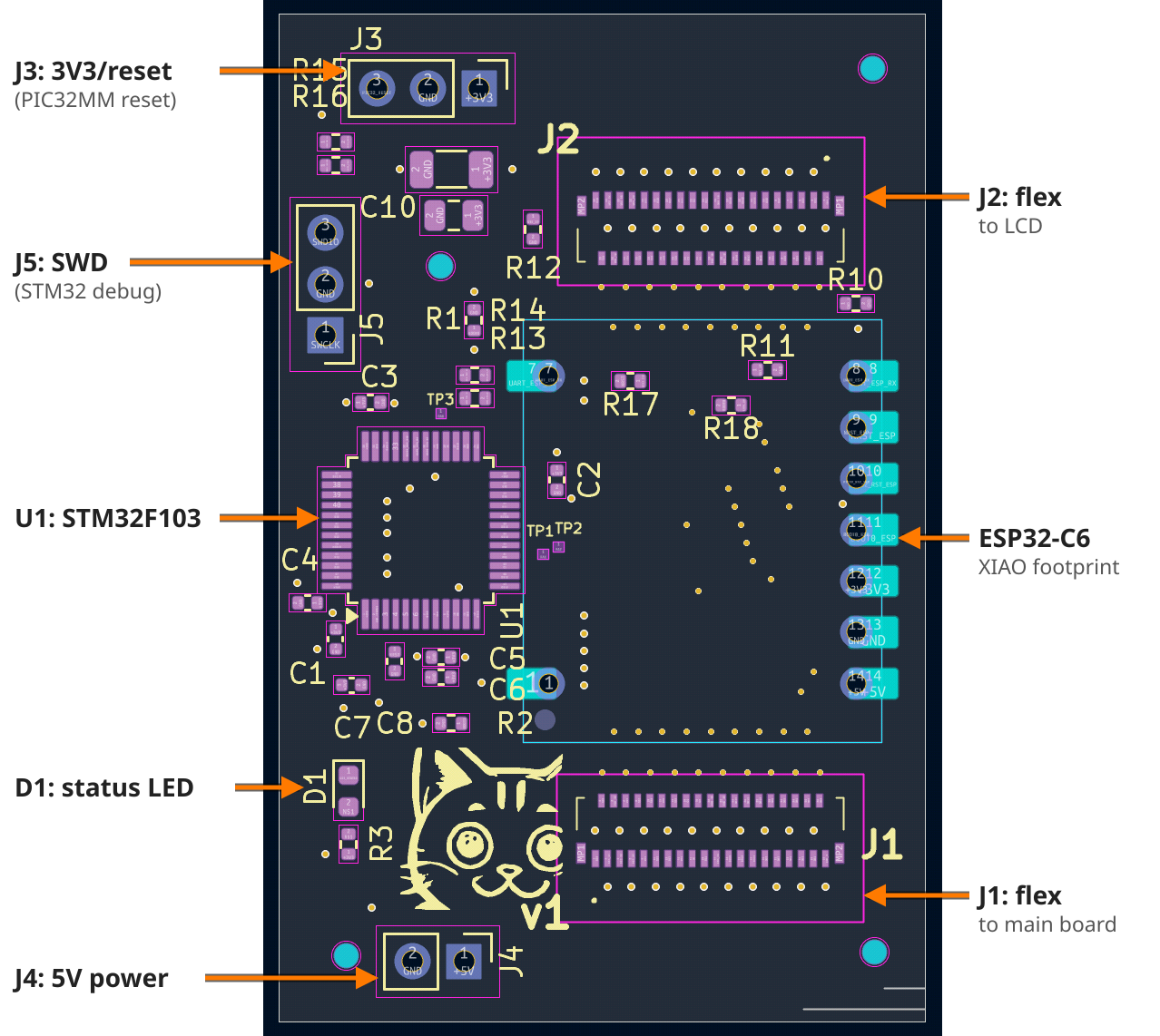
Unlike a normal EE flow, I did not spend time drawing schematics. This is probably acceptable for a one-person project: I reviewed and made changes to the design/pinout as I placed and routed components. I’m not completely sure how that would scale for larger projects.
Iterating from the design doc/SKiDL is fairly easy: prompt Claude to update both, regenerate the netlist, then just press File->Import->Netlist in KiCad. KiCad then smartly adjusts connections and components, and in the worst case, DRC checks will fail.
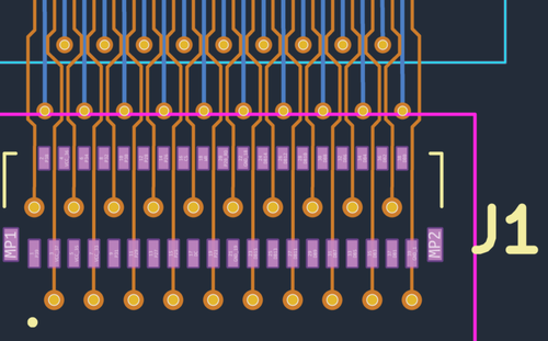
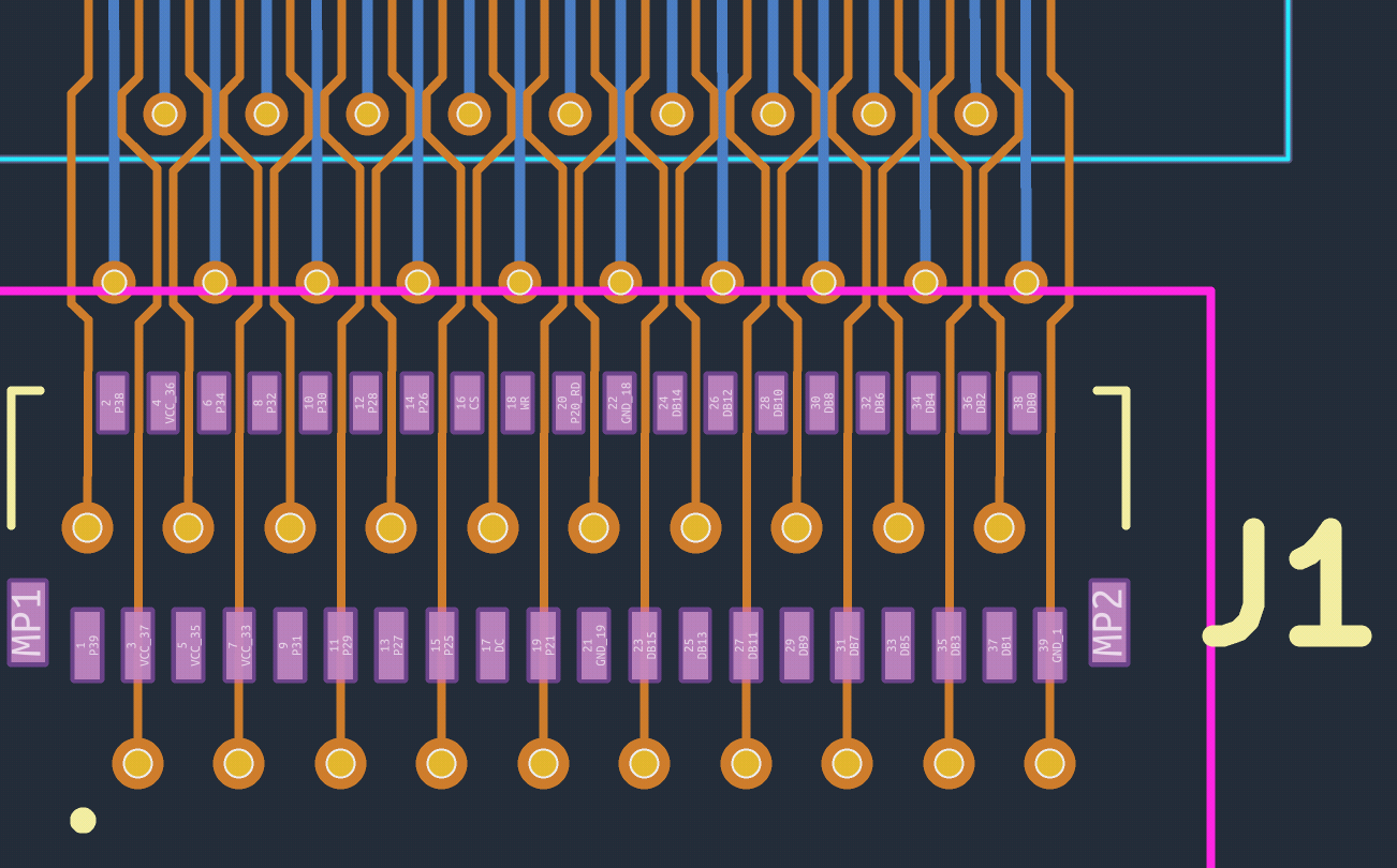
Display connector lane and tap routing
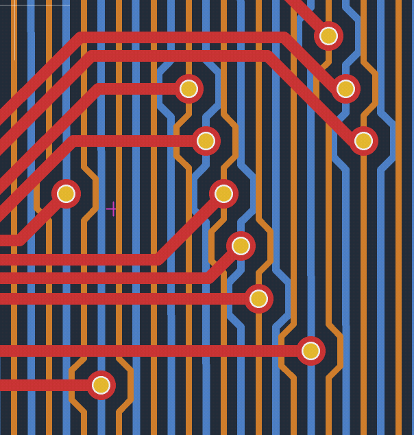
Doing most of the routing by hand was somewhat okay, and not too repetitive for this human. However, connecting the two 39-pin connectors (J1 and J2 above), with the required vias to avoid violating DRC rules, and the required 19 taps to the STM32, became extremely tedious.
Basically, routing the 39 pins between the connectors is a repeated pattern. We route the top layer pins (the connectors’ pads) to 2 other layers (we have 4 in total). The tricky bit is that we need to add “kinks” to the traces around the vias to avoid violating design rules.
We also need to add additional vias to tap the lines and connect them to the STM32. Similarly, the vias require kinks in the lines in the 2 other layers.
I asked Claude to help, and it came up with this horrible horrible thing, basically doing some glorified string replacement directly into the PCB layout file. Iterating on this was reasonably easy though: run script, press File -> Revert on KiCad, inspect, laugh at Claude silliness, ask it to fix stuff (or just start from scratch), iterate.
I selected the exact placement of the vias, tweaking the STM32 pin assignments to make routing easier, as we have facilities in the software to swap bits of the captured data anyway.
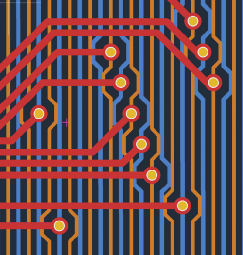
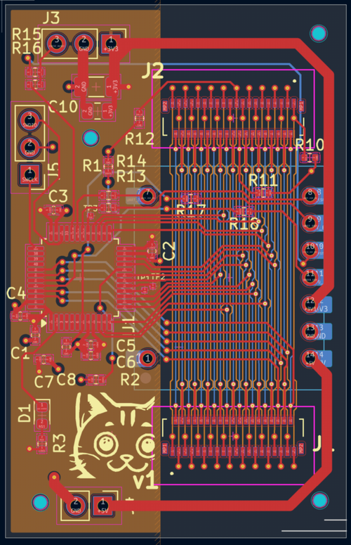
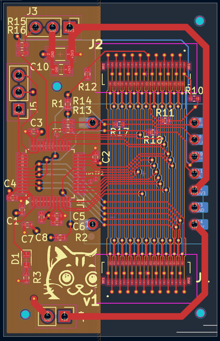
The final, routed, PCB, looks like this. This is a 4-layer PCB (2 layers would never have fit this).
Manufacturing and assembly
Confident enough, I then pressed the button on the JLCPCB website, paid a whopping 21.16 USD for 5 boards (with shipping), and waited a week.
Then I got the boards, assembled everything, and started scratching my head… Something looked very wrong in the capture, with such strange behaviour that I went down a rabbit hole trying to figure out if the STM32 I used for prototyping was a genuine part (and whether the presumably genuine JLCPCB part was actually underperforming).
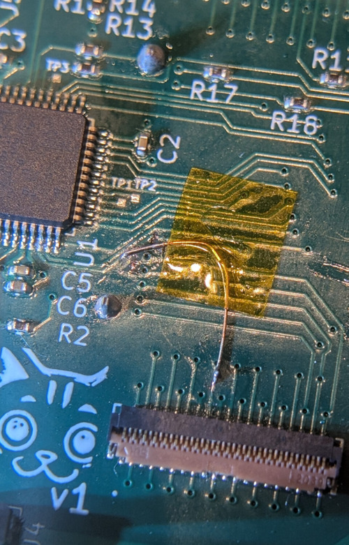
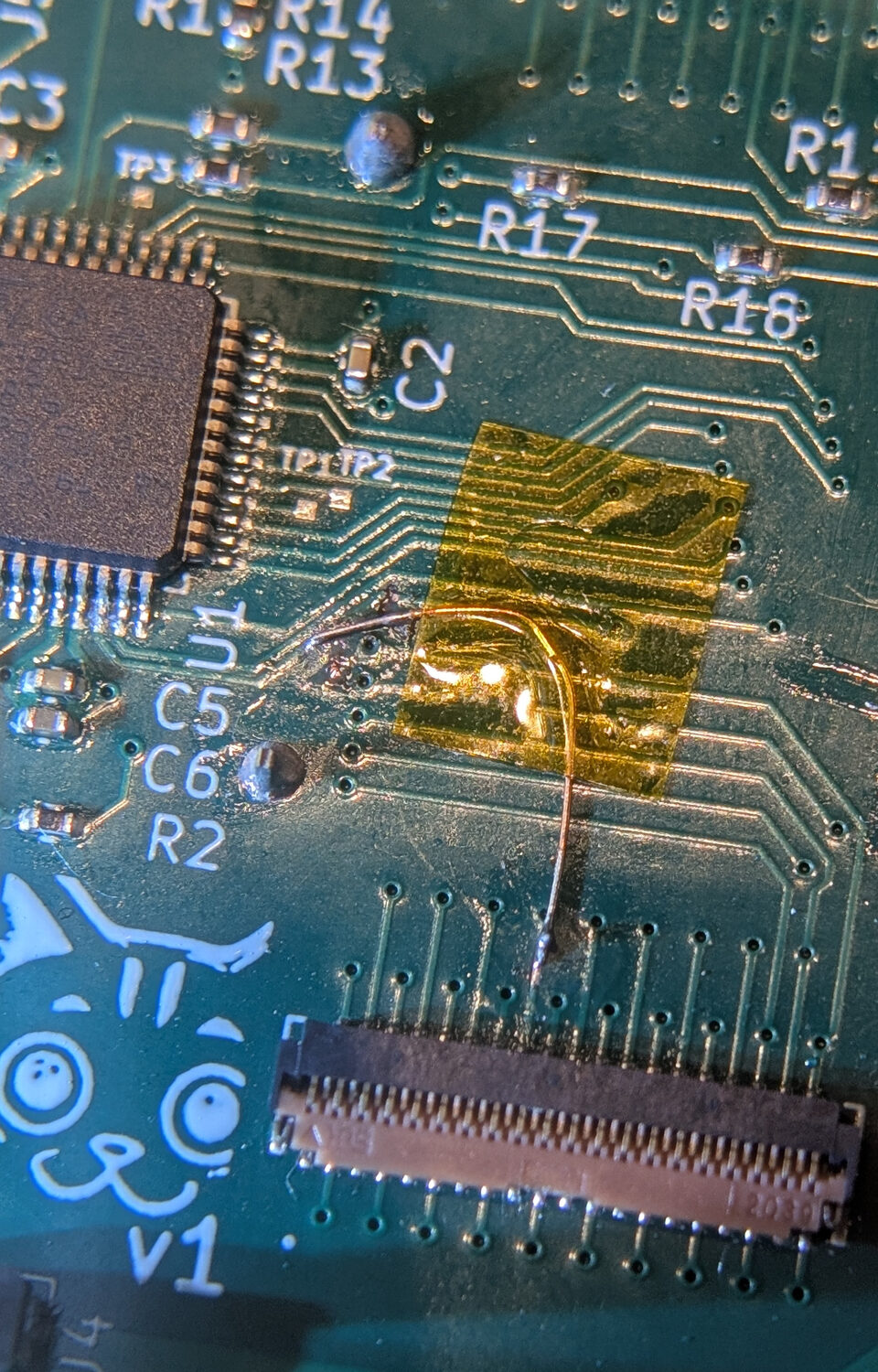
Turns out, CS and WR got swapped. I think this came from a mix-up during my reverse engineering, which I did not re-check carefully once I found the LCD spec (or, I just forgot to prompt Claude to be “extra careful”). WR is the worst pin to swap, as it is the trigger for the data capture. Luckily though, CS is not actually used, so I just cut that trace, and jumped a wire from the actual WR. Claude wrote a short erratum, and well, I guess it’s my fault, or, anyway, I’m ultimately responsible!
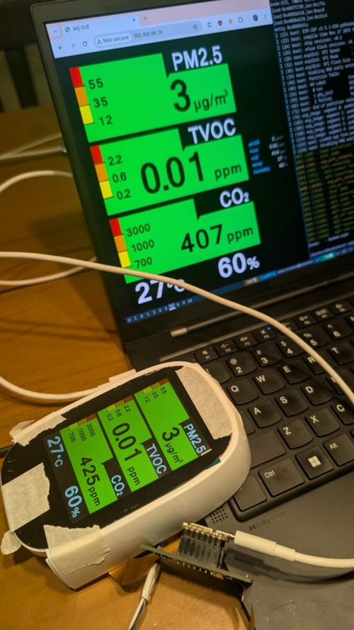
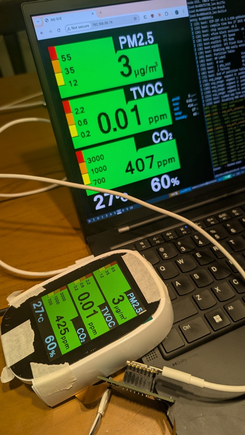
And finally, a fully working version. The ESP32-C6 runs a web server you can see displayed on the laptop, showing a mirror of the physical display, with the values decoded.
The next post will (likely) look at the firmware implementation details, and Home Assistant integration.